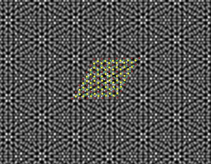
Dative Epitaxy - Growing Semiconductor Materials on vdW Templates
This is a distinct form of thin film epitaxy utilizing dative bonds used to grow semiconductor crystals with single unit cell thickness on a thin layer vdW template.
Two-dimensional (2D) semiconductors are the core force of next-generation electronics and optoelectronics, which are expected to exhibit quantum effect and greatly improve the density of the transistor, extending Moore's law.
This University at Buffalo technology relies on two step chemical vapor deposition (CVD) or physical vapor deposition (PVD) process: first, a atomically thin layer of vdW material (such as WSe2 or NbSe2) is deposited, and serves as a template. Second, a covalent semiconductor such as CdSe or GaN can be deposited. Dative epitaxy is distinctly different from conventional three-dimensional epitaxy with strong covalent bonding or conventional vdW epitaxy with strong covalent bonding or conventional vdW epitaxy where the epilayer has weak interactions with the vdW substrates. Multiple layers of Ag-SiO2 nanocomposite films are stacked to construct a graded nanomaterial ("GNM") film on a substrate (e.g., glass, polymer, fabric, etc.). The mixture ratio of Ag-SiO2 may be tuned to control the effective refractive index of the film. By controlling parameters of the film, such as the number of layers and the total thickness of the film. By controlling parameters of the film, such as the number of layers and the total thickness of the GNM, one can obtain different colors. The thermal emission of such films is weak.

This approach has been shown to be more scalable than restacking and creates less defects than chemical vapor deposition.
The subject invention has been tested to create Cr5Te8/WSe2 heterostructures and Cr2Se3/WSe2 heterostructures. There are numerous other structures that could be created starting with any vdW template. These structures have future applications in quantum computing and photonics.
PCT/US2023/063610 filed March 2, 2023.
TRL 6
Available for license or collaboration.
Patent Information:
| App Type |
Country |
Serial No. |
Patent No. |
Patent Status |
File Date |
Issued Date |
Expire Date |
|